- 您现在的位置:买卖IC网 > Sheet目录1992 > DAC5674IPHPG4 (Texas Instruments)IC DAC 14BIT 400MSPS 48-HTQFP
DAC5674
SLWS148A SEPTEMBER 2003 REVISED OCTOBER 2005
www.ti.com
13
DETAILED DESCRIPTION
Figure 1 shows a simplified block diagram of the DAC5674. The CMOS device consists of a segmented array
of PMOS current sources, capable of delivering a full-scale output current up to 20 mA. Differential current
switches direct the current of each current source to either one of the complementary output nodes IOUT1 or
IOUT2. The complementary output currents thus enable differential operation, canceling out common mode
noise sources (digital feedthrough, on-chip, and PCB noise), dc offsets, even-order distortion components, and
increase signal output power by a factor of two.
The full-scale output current is set using an external resistor RBIAS in combination with an on-chip band-gap
voltage reference source (1.2 V) and control amplifier. The current IBIAS through resistor RBIAS is mirrored
internally to provide a full-scale output current equal to 32 times IBIAS. The full-scale current can be adjusted
from 20 mA down to 2 mA.
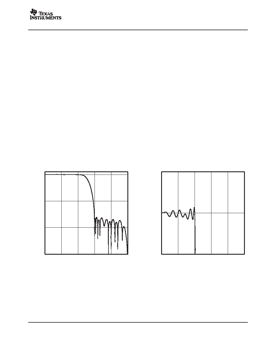
Interpolation Filter
The interpolation filters FIR1 and FIR2 can be configured for either low-pass or high-pass response. In this way,
higher order images can be selected. Table 1 shows the DAC IF output range for the different filter response
combinations, for both the first and second Nyquist zone (after interpolation). Table 2 lists the DAC IF output
ranges for two popular GSM data rates. Table 3 shows the W-CDMA IF carrier center frequency for an input
data rate of 61.44 MSPS and a fundamental input IF of 15.36 MHz. Figure 15 shows the spectral response;
the corresponding nonzero tap weights are:
D [5, 20, 50, 108, 206, 361, 597, 947, 1467, 2267, 3633, 6617, 20746, 32768]
f / fin
150
100
50
0
0.0
0.2
0.4
0.6
0.8
1.0
Amplitude
dB
AMPLITUDE
vs
FREQUENCY
f / fin
0.0
0.2
0.4
0.6
0.8
1.0
0.005
Amplitude
dB
AMPLITUDE
vs
FREQUENCY
0.005
0.000
Figure 15. FIR1 and FIR2 Magnitude Spectrum
发布紧急采购,3分钟左右您将得到回复。
相关PDF资料
DAC7621EBG4
IC SNGL 12BIT PARALLEL D/A 20SSO
DAC7801KPG4
IC DUAL 12BIT CMOS DAC 24-DIP
DAC8043AESZ
IC DAC 12BIT MULT SRL INP 8SOIC
DAC8043GP
IC DAC 12BIT MULTIPLY CMOS 8-DIP
DAC8221GP
IC DAC 12BIT DUAL W/BUFF 24-DIP
DAC8222GPZ
IC DAC 12BIT DUAL W/BUFF 24DIP
DAC8229FSZ-REEL
IC DAC 8BIT DUAL V-OUT 20SOIC
DAC8248FS
IC DAC 12BIT DUAL W/BUFF 24-SOIC
相关代理商/技术参数
DAC5674IPHP-ND
制造商: 功能描述: 制造商:undefined 功能描述:
DAC5674IPHPR
功能描述:数模转换器- DAC 14-Bit 400 CommsDAC RoHS:否 制造商:Texas Instruments 转换器数量:1 DAC 输出端数量:1 转换速率:2 MSPs 分辨率:16 bit 接口类型:QSPI, SPI, Serial (3-Wire, Microwire) 稳定时间:1 us 最大工作温度:+ 85 C 安装风格:SMD/SMT 封装 / 箱体:SOIC-14 封装:Tube
DAC5674IPHPRG4
功能描述:数模转换器- DAC 14-Bit 400 CommsDAC RoHS:否 制造商:Texas Instruments 转换器数量:1 DAC 输出端数量:1 转换速率:2 MSPs 分辨率:16 bit 接口类型:QSPI, SPI, Serial (3-Wire, Microwire) 稳定时间:1 us 最大工作温度:+ 85 C 安装风格:SMD/SMT 封装 / 箱体:SOIC-14 封装:Tube
DAC5675
制造商:TI 制造商全称:Texas Instruments 功能描述:14-BIT, 400-MSPS DIGITAL-TO-ANALOG CONVERTER
DAC5675A
制造商:TI 制造商全称:Texas Instruments 功能描述:14-Bit, 400MSPS Digital-to-Analog Converter
DAC5675AEVM
功能描述:数据转换 IC 开发工具 DAC5675A Eval Mod RoHS:否 制造商:Texas Instruments 产品:Demonstration Kits 类型:ADC 工具用于评估:ADS130E08 接口类型:SPI 工作电源电压:- 6 V to + 6 V
DAC5675AIPHP
功能描述:数模转换器- DAC 14-Bit 400-MSPS RoHS:否 制造商:Texas Instruments 转换器数量:1 DAC 输出端数量:1 转换速率:2 MSPs 分辨率:16 bit 接口类型:QSPI, SPI, Serial (3-Wire, Microwire) 稳定时间:1 us 最大工作温度:+ 85 C 安装风格:SMD/SMT 封装 / 箱体:SOIC-14 封装:Tube
DAC5675AIPHP
制造商:Texas Instruments 功能描述:IC DAC 14BIT 400MSPS 48-HTQFP